Science
Columbia Engineers Revolutionize Quantum Tech with Nanoscale Metasurfaces
A team of engineers at Columbia University has made significant strides in quantum technology by creating nanoscale metasurfaces that enhance nonlinear optical effects. This innovation is detailed in a study published in Nature Photonics in October 2025, marking a breakthrough in the efficiency of entangled photon pair generation.
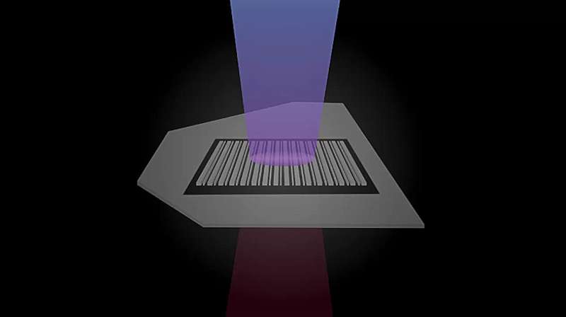
Led by Jim Schuck, a professor of mechanical engineering, the team has successfully reduced the size of nonlinear platforms to a mere 160 nanometers. This was accomplished by integrating artificial geometries into ultrathin crystals, allowing for enhanced optical properties crucial for advancing quantum technologies.
Advancements in Nonlinear Optics
The Columbia Engineering team focused on a specific class of materials known as transition metal dichalcogenides (TMDs). These materials can be thinned down to single-atom layers, offering customizable options for various applications. Despite their impressive nonlinear characteristics, traditional TMD layers were too thin to effectively generate photons at new frequencies, which is essential for practical quantum devices.
According to Chiara Trovatello, an assistant professor at Politecnico di Milano and co-author of the study, “Size doesn’t matter for something like a laser pointer that you’ll hold in your hand. But for quantum technologies, like quantum processors, size becomes crucial.” Current quantum processors require multiple qubits, which demand significant space and resources. The aim of this research is to simplify and miniaturize these sources, making them viable for widespread use.
In their previous work published in January, the team employed a technique called periodic poling, layering molybdenum disulfide in alternating directions to optimize optical output. This meticulous arrangement ensured that light waves traveling through each layer were phase-matched, preventing interference. The new research introduces a complementary approach using TMDs with tunable, etched metasurfaces.
Innovative Techniques and Future Applications
The introduction of metasurfaces allows researchers to manipulate the optical properties of materials in unprecedented ways. By strategically removing sections of atoms, the team created periodic geometries that significantly enhanced the nonlinear effects of the crystals. Ph.D. student and first author Zhi Hao Peng developed the nanofabrication technique that enabled the etching of a series of repeating lines onto molybdenum disulfide.
“Our design enhances the nonlinear effects much more than traditional linear optical optimization techniques, achieving strong enhancement not previously possible,” said Peng. The results showed an almost 150-fold increase in second-harmonic generation, a process where two photons combine to create one with double the frequency and half the wavelength.
This advancement paves the way for the team to explore the reverse process: splitting one photon into two entangled photons. Notably, Peng’s methodology is simpler and more cost-effective than previous techniques, making it easier to produce complex patterns using standard cleanroom etching technologies.
Collaborators from the CUNY Advanced Science Research Center, including Andrea Alu and former postdoctoral researcher Michele Cortufo, contributed theoretical insights that guided the metasurface design. Their work demonstrated that effective nonlinear response could be achieved through simple modifications, such as creating periodic arrangements of lines with alternating widths.
As metasurfaces have gained prominence in the field of photonics over the past decade, this research represents one of the first successful integrations with 2D crystals at such a scale. Alu emphasized the significance of this work, stating, “This work demonstrates how engineered nonlocalities in metasurfaces can unlock unprecedented nonlinear efficiencies when combined with 2D materials.”
The implications of this research extend to telecommunications, with the generated light operating at wavelengths compatible with existing networks. Schuck noted, “This could be one of the most compact sources of entangled photons at that wavelength range. With our footprint, we can really start to think about fully on-chip quantum photonics.”
In summary, the work led by Jim Schuck and his team at Columbia University not only advances the field of quantum optics but also sets the stage for more compact and efficient quantum technologies. As researchers continue to refine these techniques, the potential for scalable quantum devices becomes increasingly tangible.


Community Honors Jane Morris with Celebration of Life Service

NASA Tests Innovative CryoFILL System for Future Space Missions

CMS to Address Healthcare Fraud in Congressional Hearing
Heat Pumps Transform Heating and Cooling in Grand County

Indian River State College Hosts Free Open Houses This Spring

Louis Vuitton and Miu Miu Present Distinct Visions at Paris Fashion Week

Western Nevada College Faculty Members Awarded Tenure by Regents

Elwyn Raymond Van Enwyck, 98, Remembered for Kindness and Service

Blood Test Could Forecast Alzheimer’s Risk Up to 25 Years Ahead

Nostradamus’ 2026 Predictions: Star Death and Dark Events Loom

Breakthroughs and Challenges Await Science in 2026

OpenAI to Implement Age Verification for ChatGPT by December 2025

Electric Moto Influencer Surronster Arrested in Tijuana

Discover the Top 10 Calorie Counting Apps of 2025

Bella Hadid Shares Health Update After Treatment for Lyme Disease

Analysts Project Stronger Growth for Apple’s iPhone 17 Lineup

Top 10 Penny Stocks to Watch in 2026 for Strong Returns

Japanese Study Finds Rose Oil Can Increase Brain Gray Matter
-
 Science2 months ago
Nostradamus’ 2026 Predictions: Star Death and Dark Events Loom
-
 Science3 months ago
Breakthroughs and Challenges Await Science in 2026
-
 Technology3 months ago
OpenAI to Implement Age Verification for ChatGPT by December 2025
-
 Technology6 months ago
Electric Moto Influencer Surronster Arrested in Tijuana
-
 Technology8 months ago
Discover the Top 10 Calorie Counting Apps of 2025
-
 Health6 months ago
Bella Hadid Shares Health Update After Treatment for Lyme Disease
-
 Health6 months ago
Analysts Project Stronger Growth for Apple’s iPhone 17 Lineup
-
 Technology3 months ago
Top 10 Penny Stocks to Watch in 2026 for Strong Returns
-
 Health6 months ago
Japanese Study Finds Rose Oil Can Increase Brain Gray Matter
-

 Science5 months ago
Starship V3 Set for 2026 Launch After Successful Final Test of Version 2
-

 Education6 months ago
Harvard Secures Court Victory Over Federal Funding Cuts
-

 Health6 months ago
Erin Bates Shares Recovery Update Following Sepsis Complications